
Heterogeneous Integration of Silicon Photonics and Electrical Chips: CPO Commercialization
The semiconductor industry is entering a new phase where electrical interconnect alone is no longer enough. As AI clusters, data center switches, and high-performance networking platforms grow in scale, the old model of pushing more bits through copper traces is running into hard limits. That is where co-packaged optics, or CPO, comes in. By bringing silicon photonics and electrical chips into the same advanced package, CPO offers a practical path to higher bandwidth density, lower power consumption, and better scalability for the systems that move the world’s data.
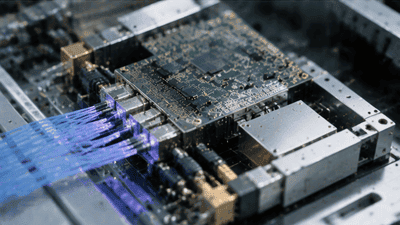
What makes this moment especially interesting is that CPO is no longer just an elegant research idea. It is entering commercialization, which means the real questions are no longer “Can it work?” but “How do we manufacture it, qualify it, and scale it economically?” That shift places heterogeneous integration at the center of the story. The challenge is not only to design a good photonic engine or a strong electrical chip, but to make them coexist in a package that can survive heat, assembly stress, and the unforgiving economics of mass production.
Why CPO Exists
Modern data centers and AI infrastructure are hungry for bandwidth. Traffic growth inside data centers has been rising rapidly, and a large share of that traffic never leaves the building, which means the problem is not just long-distance communications but the local movement of enormous amounts of data between compute, memory, and switching fabrics. Traditional pluggable optics have done a remarkable job, but they are beginning to struggle with power, size, and signal integrity as link speeds climb.
CPO addresses that by moving optics closer to the electrical chip. Instead of driving electrical signals over long board traces to a separate optical module, the optical engine is co-packaged with the switch ASIC, accelerator, or other electrical logic. That shortens the electrical path, reduces power loss, and opens the door to higher bandwidth density. It also changes the packaging game entirely, because optics and electronics now have to be integrated as one system rather than two separate components.
What Heterogeneous Integration Adds
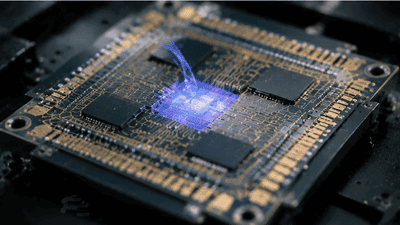
The magic phrase here is heterogeneous integration. CPO is not simply “a photonic chip plus an electrical chip.” It is a carefully engineered package in which different functions, process technologies, and material systems are brought together to behave like one coherent platform. The photonic integrated circuit, or PIC, may be fabricated in a silicon photonics process. The electrical chip may come from a leading CMOS node. Lasers, drivers, modulators, detectors, and control logic may all live in the same broader package ecosystem.
That combination is powerful because each piece can be optimized for its own job. Silicon photonics is ideal for compact optical routing and wavelength multiplexing, while advanced CMOS is ideal for high-speed electronics and control. But the package must bridge the two worlds with very short, clean interconnects and a thermal strategy that keeps both sides stable. In other words, the success of CPO depends as much on advanced packaging as it does on photonics design.
The Packaging Challenge
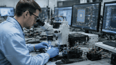
Commercializing CPO sounds straightforward on paper: put the optical engine next to the ASIC, connect them tightly, and ship. In practice, the packaging challenge is where most of the difficulty lives. The optical engine and the electrical chip do not just need to be electrically connected. They need to be aligned, thermally managed, mechanically protected, and assembled with high yield. Even minor misalignment can affect optical coupling efficiency, while small variations in package stress can degrade reliability or performance.
The package has to support multiple sensitive elements at once. The photonic portion may be sensitive to temperature drift and alignment tolerances. The electronic portion may generate significant heat. The substrate must support high-density routing while maintaining signal integrity. And if the design includes integrated laser sources or hybrid optical elements, the packaging difficulty rises further. CPO is therefore a textbook example of why heterogeneous integration is no longer a niche discipline; it is becoming a mainstream system design requirement.
Electrical and Optical Trade-Offs
One reason CPO is so attractive is that it changes the economics of data movement. Copper interconnects consume more power and become less practical as distance and speed increase. By shifting the optical conversion point closer to the ASIC, CPO lowers the electrical reach requirement and helps cut the energy per bit. The system can use optics for the long or bandwidth-heavy paths, while keeping the electrical portion short and efficient.
At the same time, the package cannot be optimized for optics alone. Electrical chips still need robust power delivery, clean timing, low-jitter drivers, and fast control logic. The PIC may benefit from compact waveguides and wavelength-division multiplexing, but the electrical interfaces still need to be stable and manufacturable. This is what makes CPO different from a simple module swap. The electrical and optical sides must be co-designed from the beginning, or the gains disappear in packaging overhead.
Thermal Management Becomes Central
If there is one issue that keeps coming up in CPO commercialization, it is heat. Optical engines do not like uncontrolled temperature variation, and electrical ASICs often run hot, especially in high-end switching and AI environments. When the two are placed in close proximity, thermal design becomes mission-critical.
This has pushed advanced packaging teams to rethink everything from heat spreaders to substrate layout. Some architectures place the optical engine near the perimeter of the package to keep it away from the hottest zones. Others use separate thermal paths or dedicated cooling structures so that the photonic components remain stable. In a commercial product, thermal drift is not just a lab curiosity; it can affect link budget, wavelength tuning, reliability, and long-term field performance.
That is why CPO commercialization is inseparable from advanced encapsulation. The package must protect, isolate, and cool in ways that are compatible with both the optics and the electronics. It is a balancing act, and the balance is delicate.
What Makes CPO Commercialization Hard
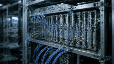
Commercialization brings a completely different set of priorities than a prototype demonstration. A demo can tolerate special handling, custom assembly, and a low production rate. A commercial platform must survive yield pressure, supply chain variability, and customer qualification. That means the package has to be repeatable, scalable, and cost-justified.
Several issues stand in the way:
- Yield. The more components you co-package, the more opportunities there are for assembly or alignment defects.
- Supply chain complexity. CPO may involve separate semiconductor, photonics, laser, substrate, and packaging partners.
- Test complexity. Optical and electrical test flows must be integrated and efficient enough for production.
- Assembly precision. Optical coupling requires extremely accurate placement and stable mechanical structures.
These are not trivial hurdles. They explain why CPO has taken longer to commercialize than many expected. The concept is strong, but the industrialization path is more difficult than a traditional electrical package because the system is inherently mixed-technology.
Where the Market Is Starting
CPO is most compelling in high-bandwidth, power-sensitive environments such as data center switching and high-performance interconnect fabrics. That is where the value proposition is clearest: less power spent on electrical signal driving, better bandwidth density, and more scalable architecture as switch speeds rise.
In that context, the first commercial products are likely to focus on the most bandwidth-constrained, high-value platforms. These systems can justify the packaging complexity because the cost of not solving the interconnect problem is even higher. Over time, if the packaging and yield issues continue to improve, the technology could spread into other optical interconnect markets as well.
But the initial commercialization wave will almost certainly be selective. CPO will not replace all pluggable optics overnight. Instead, it will enter the market where the economics and the bandwidth needs align most strongly.
Advanced Packaging Platforms Matter
One of the reasons CPO is moving toward commercialization now is that advanced packaging platforms themselves have matured. Technologies such as chip-on-wafer-on-substrate, fan-out, and 3D integration provide a toolkit for bringing electrical and optical chips closer together in a controlled, manufacturable way.
In practical terms, the package may include:
- A switch ASIC or accelerator chip built on a leading-edge CMOS node.
- An optical engine containing the PIC and associated drivers or modulators.
- A high-density substrate or interposer that routes signals cleanly between them.
- Thermal structures that keep the optical side stable and the electrical side cool.
That is classic heterogeneous integration: multiple specialized dies, different process technologies, one package. The advanced packaging platform becomes the glue that allows the whole system to function as a commercial product.
Standardization and Ecosystem Pressure
For CPO to scale, the ecosystem will need more than just one good package. It will need some level of standardization across interfaces, assembly methods, and test flows. That includes photonic electrical interface conventions, package reliability expectations, and interoperability between optical engine suppliers and electrical chip vendors.
The reason is simple: if every CPO module is completely custom, it will be hard to scale production or reduce costs. Standardization does not need to eliminate innovation, but it does need to create repeatable building blocks. That is especially important in heterogeneous integration, where the number of variables can grow quickly once photonics enters the package.
In that sense, CPO commercialization is not only a technical milestone. It is also a coordination problem. The companies that align chip design, packaging, materials, and test will have a much smoother path to volume.
What Success Looks Like
A successful CPO product does not necessarily look flashy from the outside. It looks like a package that:
- Delivers the expected bandwidth at acceptable power.
- Maintains stable optical performance under real thermal conditions.
- Qualifies for reliable manufacturing at volume.
- Fits into the customer’s data center, accelerator, or switching architecture without a major redesign.
That may sound modest, but in advanced packaging terms it is a major achievement. It means the package has moved from experimental integration to production-ready heterogeneous assembly. It means photonics is no longer adjacent to the compute system. It is part of the compute system.
The Road Ahead
The next few years will likely determine whether CPO becomes a broad commercialization success or remains a high-value niche. The drivers are strong: AI and HPC demand more interconnect bandwidth than copper can comfortably provide, and power efficiency is becoming a board-level priority in data centers. At the same time, packaging, yield, and thermal obstacles remain real.
If the industry can keep improving heterogeneous integration flows, CPO could become one of the most important packaging transitions of the decade. It would shift more of the interconnect burden from electrical traces to optical links and push advanced packaging deeper into the heart of data infrastructure. That would be a significant change, not just for optics companies, but for the entire semiconductor packaging ecosystem.
Conclusion
CPO commercialization is really a story about advanced packaging becoming the enabler of a new kind of system design. Silicon photonics and electrical chips are each powerful on their own, but the real value emerges when they are tightly integrated into one package and supported by a mature heterogeneous integration flow. That package has to solve electrical, optical, thermal, mechanical, and manufacturing challenges all at once.
That is why CPO matters so much. It is not just a faster link or a clever package trick. It is a sign that the semiconductor industry is moving into an era where optics and electronics are designed together, packaged together, and commercialized together. In that world, advanced encapsulation is not the last step of the process. It is the place where the system becomes real.





